Tin Surfaces
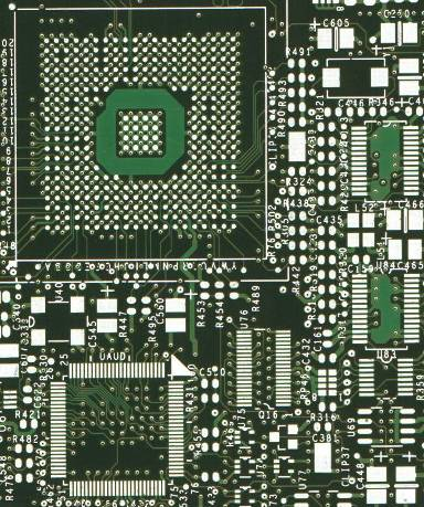
Immersion tin is established as a planar, lead-free and multi-solderable surface. Press-fit technology as well as conductive bonding with suitable adhesives are also possible. Some CIF connectors are equipped with tin-plated contacts. In these cases, the data sheets also recommend chem. Tin is recommended.
The wettability of chem. tin is comparable to chem. Ni/Au. Solder propagation and solder penetration through vias, on the other hand, is better than with chem. Ni/Au. Compared to HAL, the wettability is somewhat worse, since the tin itself does not melt over the entire surface due to its low layer thickness.
The higher and denser the tin layer grows on the copper, the lower the exchange rate becomes. This means that at a tin layer thickness of approx. 1 µm, further tin can only be deposited very slowly. However, the process time in the electroless tin bath is limited not only for economic reasons. Solder resist does not withstand the process load indefinitely.
The coating thickness should be >1 µm in order to reliably perform multiple lead-free soldering operations. Good timing of the soldering processes is important for this.
The storage time for electroless tin is 6-12 months, depending on the subsequent surface requirements. If several unfavorable conditions come together, other surfaces may be more suitable. The following points can negatively influence the solderability:

More Tin Surfaces
Hot Air Leveling (HAL, Hot Air Solder Leveling, HASL, hot air tinning) was the most commonly used surface until IEEE/RoHS came into effect in mid-2006. It has excellent soldering properties and can be stored for longer than 12 months.
Due to the lead ban, much of the hot tinning is now done with lead-free solders. However, most HAL applications have now been switched to chem. Tin or chem. Ni/Au, since the HAL surface is not panaric and can only be processed with uncertainties for fine-pitch devices and BGAs. Furthermore, the thermal stress on the PCBs is so high, especially with HAL lead-free, that the failure rates for non-standard PCBs increase. The use of modern materials (phenolic hardening, ceramic-filled, medium Tg) has more than compensated for this shortcoming in HAL lead-free.
Further Tin Surfaces
Special technology: Electroplated Ni/SnPb
A special technology for reliable and long-term stable surfaces is the galvanic Ni/SnPb surface (Ni/TinPad). Here, a galvanic nickel layer is located between copper and solder.
Special technology: tin/lead remelted/refused
For these historic surfaces, the tin/lead layer deposited as an etch resist is heated briefly above the melting point in an infrared reflow furnace. This both encloses and protects the flanks of the conductors from solder and transforms the rough galvanic metal structure into a smooth eutectic one, which is less susceptible to corrosion.
With the introduction of solder resist, this surface has almost disappeared. The process has the disadvantage that the Sn/Pb melts under the solder resist and the resist becomes wavy there (so-called orange peel effect).
Special technology: Hot-oil leveling
Similar to hot-air leveling, hot-oil leveling (hot oil tinning) involves immersing the circuit boards in the liquid tin-lead bath. To remove excess tin from the surface and from the holes, hot oil, which is an oil bath above the tin bath, is pumped through nozzles against the circuit board. Process control problems caused this surface to disappear in favor of HAL.
Special technology: roll tinning/roll tinning
In horizontal roll tinning, the printed circuit boards are shot through up to 3 pairs of rolls after fluxing at a speed of 5 – 30 m/min. and then blown out. The contact times with the solder are approx. 1 – 2 sec. Flexible printed circuit boards are still partially roll-tinned today.
For further questions regarding tin surfaces, please contact our technology manager Dr. Lehnberger:

You are currently viewing a placeholder content from Google Maps. To access the actual content, click the button below. Please note that doing so will share data with third-party providers.
More InformationANDUS ELECTRONIC
LEITERPLATTENTECHNIK
Receive helpful tips on all aspects of printed circuit boards and interesting news from ANDUS.
We have sent you a confirmation email. Please click the confirmation link in it to confirm your registration.

Unser Technologieleiter, Herr Dr. Lehnberger, wird Ihnen am 10.06. und 12.06. einen Einblick in die Besonderheiten beim Einsatz von Langflex-Leiterplatten geben.

Unser Technologieleiter, Herr Dr. Lehnberger, wird Ihnen am 08.04. und 10.04. einen Einblick in FR4-Material geben.

Unser Technologieleiter, Herr Dr. Lehnberger, wird Ihnen am 19.08. und 21.08. einen Einblick in Hochfrequenz-Leiterplatten und Impedanzkontrolle geben.


You need to load content from reCAPTCHA to submit the form. Please note that doing so will share data with third-party providers.
More InformationYou are currently viewing a placeholder content from MailerLite. To access the actual content, click the button below. Please note that doing so will share data with third-party providers.
More InformationYou need to load content from reCAPTCHA to submit the form. Please note that doing so will share data with third-party providers.
More InformationYou are currently viewing a placeholder content from Turnstile. To access the actual content, click the button below. Please note that doing so will share data with third-party providers.
More Information